

By Andrea Vinci
The advent of SiC and GaN MOSFET technologies is driving a disruptive revolution in the power electronics industry. These new materials permit efficiency percentages, for the entire conversion system, that were simply unimaginable a few years ago.
There is no such thing in the real world as an ideal switching characteristic, but several classes of wideband gap devices based on the new materials are emerging with extremely low switching losses. The combination of low switching losses and the ability to deal with very high dv/dt slew rates and support for very fast switching frequencies, make the new technologies the dream -- and the nightmare -- of the DC/DC converter design engineer all at the same time.
Let’s consider a design engineer working on a power conversion application, such as an inverter or a motor drive controller, or one who is taking on the challenge of designing a power factor correction (PFC) circuit that pushes power supply efficiency above the 99 percent limit. What challenges do they face?
Using a low loss transistor is just the beginning of the steep mountain they must climb. A fully isolated gate driver circuit must be able to properly drive and control the power stage which in turns leads to several issues that must be solved, ranging from isolation to the need for circuit protection techniques to avoid the potential catastrophe of the so-called “feed-through” problem.
When designing high frequency converters, a large portion of design time must be spent on simulation and verification to confirm that all possible causes of failure have been considered and addressed. A talented PCB designer can perform magic with the layout, but the parasitics are still there, lurking around corner. This alone can keep design teams busy and as they accumulate experience with new device packages, new system layouts and new topologies. Indeed, the move to new SiC and GaN devices adds new complications.
Getting the most out of the new devices
The fil rouge or common thread across the PFC/power supply market, the PV inverters market and the automotive market as well as the consumer wireless charging applications is the desire to get the most out of SiC and GaN technologies.
Certainly, the requirements among these various application systems differ considerably. What a designer requires from a semiconductor device in terms of electric field magnitude, on-resistance or blocking voltage can force the move into a very specific and narrow swim lane. But there are common issues facing both a 20kW electric car battery charger designer using SiC at 250kHz and resonant topology designers of GaN-based wireless power designs working at 6.78MHz.
In both cases, the designers have a need to clearly characterize static and switching losses with high accuracy. They all need to deal with and properly manage heat dissipation and to quantify the cooling medium. They both likely have new generation transformers, inductors and capacitors catalogs on their desk that they may have never used before. They also are worried that the soldered in probe access wire could act as a mini antenna when EMC characteristics must be verified.
They also are starting to recognize that the instrumentation toolkit they used in the past may not be sufficient for what they need to do now. Devices need to be tested for breakdown up to thousands of volts and at the same time vetted for leakage currents that can be as low as femto-amps. Are the power sources, the multimeters and the oscilloscopes still up to the task?
With all these MOSFET Vgs and Vds and currents that have to be simultaneously measured, with precise skew characterization, can they still use their four channel scopes with some external signal trick to achieve synchronization? How much time should they invest in post processing the waveforms and putting it all together offline to form decisions over the circuit behavior? Do they have enough sensitivity for the gate threshold voltage measurement on their old scope, and the oscillations they keep tracking on the scope screen, are they real or coming from the probe leads?
Invariably, SiC and GaN, designers almost universally tick off several pain points and measurement challenges including:
- High dv/dt, high di/dt and high switching frequencies that create issues related to EMI
- Measuring low voltages in the presence of high common mode current
- High voltage overshoot
- Cross-talk and other headaches in PCB layout design
- Determining what percentage of the errors are coming from the measurement system
The Vgs measurement problem
Another area where designers struggle involves measuring Vgs in topologies called phase-leg or half-bridge configurations, as shown in Figure 1.
In this configuration, when one SiC MOSFET turns on, the very high dv/dt induces spurious voltage on the gate to source voltage (Vgs) of the complementary MOSFET as shown in Figure 2. This reduces signal to noise margin on this latter Vgs making it prone to spurious turn-on.
Of course, you do not want to lower dv/dt, since this high slew rate is what allows these devices to achieve such minimal switching losses. Therefore, the problem must be solved differently, for example, by working on the gate driver side to actively control gate resistance of the two stages in the switching process.
In addition, an extremely talented PCB designer must make sure that the bus and connecting lanes have minimal inductive effect so as to not contribute too much to voltage and overshoot ringing caused by inductive loops. All these elements must be validated with real circuit simultaneous measurements of high side and low side stages Vgs to characterize pulse width modulation (PWM) delay time and minimize dead time to increase performances. You then need to measure the currents, and the two Vds for complete loss characterization.
Four channels scopes are insufficient for this job, and typical 8-bit ADCs do not provide sufficient vertical resolution. Also, the common probes in most lab drawers have now proven to be inadequate, even good differential probes that have traditionally proved to be sufficient for making floating measurements on the high side stage. Traditional differential probes are based on differential amplifiers which are connected to earth ground. This ground connection limits the common mode voltage range, causes common mode voltage frequency derating, creates ground loops, and limits the common mode rejection.
Fortunately, just as there’s a disruptive revolution with the emergence of wideband gap devices there’s also a disruptive revolution going on among power efficiency measurement solutions.
New measurements solutions
A typical measurement system in this space is based on oscilloscopes and differential probes that provide the connection between the device under test (DUT) and the oscilloscope. Scope selection is critical in terms of appropriate bandwidth, noise floor, vertical resolution, number of channels and application software versatility. Probe selection is critical because probe performance can be the limiting factor in the measurement system.
When a differential measurement is needed, conventional differential probes as mentioned earlier often fail to provide a good representation of the actual signal due to limitations in their common mode rejection ratio, derating over frequency, frequency response, and the parasitics introduced by probe’s input leads. These limitations become more pronounced when testing SiC and GaN power devices with very fast switching rates and high nominal common mode voltage.
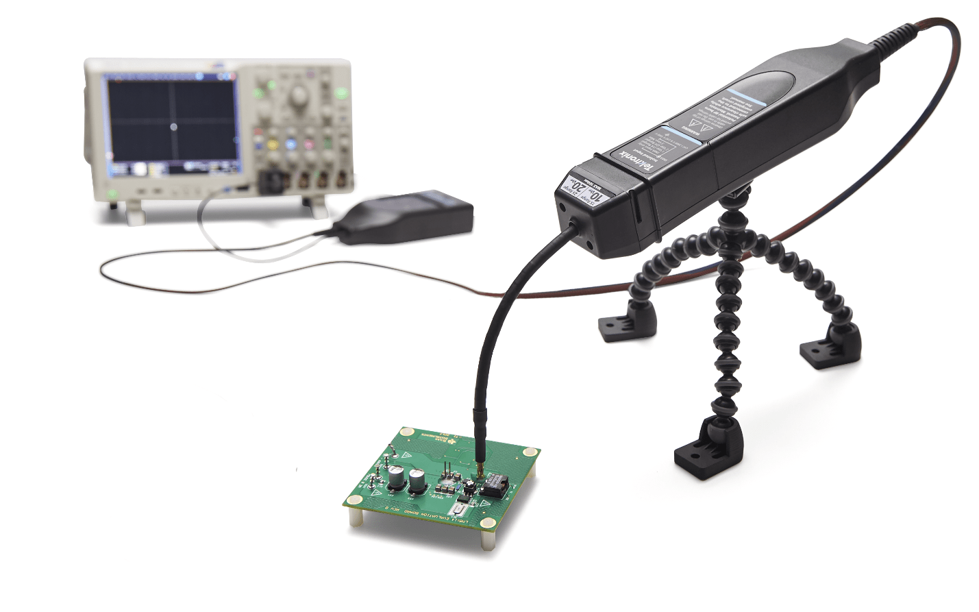
Since the problem of capturing these signals stems from the need for earth ground, it follows that a workable solution would be probe technology that does not depend on earth ground, and therefore would be more or less immune to the effects of high-common mode voltage. Such a system now exists in the form of the patented IsoVu measurement system from Tektronix, which operates entirely through fiber optics.
The IsoVu measurement system is a leap forward for Vgs measurements and is the only solution with the required combination of high bandwidth, high common mode voltage, and high common mode rejection to enable the differential measurements required for new applications involving wide bandgap MOSFETs. IsoVu offers complete galvanic isolation from the DUT and uses an electro-optic sensor to convert the input signal to optical modulation, which electrically isolates the DUT from the oscilloscope.
The sensor head, which connects to the test point, has complete electrical isolation and is powered over one of the optical fibers. The probe tips are designed to be shielded all the way to the tip and minimize parasitics. The probe is not only offers significant advantages for power conversion testing but is also well suited for stringent EMI and ESD test requirements.
Unlike electrical probes that should be kept as short as possible, cable length is not an issue for measurement systems based on fiber optics. Remote measurement capability can be very useful when the DUT and the oscilloscope must be (or should be) kept some distance apart from each other.
The IsoVu system works with most Tektronix scopes, but the best combination comes when it is used in combination with the 12-bit vertical resolution of the new 5 Series MSO oscilloscopes that offer up to 8 analog channels in a single unit and advanced power application software. This combination enables designers to finally take advantage of everything the wide bandgap materials have to offer for DC to DC power converters, but also represents a significant advance for 3-phase power electronics, power supply design, automotive electronics and much more.
About the Authors
Andrea Vinci is a Business Development Manager at Tektronix – Keithley in EMEA. He has an M.Sc.from Università di Padova – Italy.in Electronic Engineering.